Tamper-Sensing Meshes in the Wild
jaseg
Gulaschprogrammiernacht 24 (GPN24) · Day 2 · ZKM Kubus
Overview
In "Tamper-Sensing Meshes in the Wild," jaseg, a PhD candidate specializing in hardware security, presents an exhaustive analysis of tamper-sensing meshes—a critical, yet often overlooked, component of physical security in electronic devices. The talk delves into the practical implementation, observed vulnerabilities, and design recommendations for these ubiquitous security features. Tamper-sensing meshes are essentially looped conductors, typically embedded within circuit boards or flexible circuits, designed to detect physical intrusion attempts such as drilling, sawing, or prying. Upon detection, these meshes trigger an immediate, often destructive, response like key deletion, alarms, or device shutdown, thereby safeguarding sensitive data and functionality.
Key moments
- 0:40 What are tamper sensing meshes and their uses?
- 4:00 Survey of real-world mesh implementations
- 7:15 Creative 3D and connection methods
- 10:30 Common security vulnerabilities observed
- 12:30 Key design recommendations for security meshes
- 14:00 Advanced strategies for robust tamper sensing
- 17:00 How meshes are monitored and bypass challenges
Tamper-Sensing Meshes in the Wild
Speakers: jaseg, PhD Candidate in Hardware Security
Conference: GPN24
YouTube: https://www.youtube.com/watch?v=ck6ydzyJST4
Overview
In "Tamper-Sensing Meshes in the Wild," jaseg, a PhD candidate specializing in hardware security, presents an exhaustive analysis of tamper-sensing meshes—a critical, yet often overlooked, component of physical security in electronic devices. The talk delves into the practical implementation, observed vulnerabilities, and design recommendations for these ubiquitous security features. Tamper-sensing meshes are essentially looped conductors, typically embedded within circuit boards or flexible circuits, designed to detect physical intrusion attempts such as drilling, sawing, or prying. Upon detection, these meshes trigger an immediate, often destructive, response like key deletion, alarms, or device shutdown, thereby safeguarding sensitive data and functionality.
The significance of this research lies in its empirical approach, moving beyond theoretical discussions to dissect real-world applications. Jaseg and their team conducted a comprehensive survey by acquiring and disassembling electronic waste, including payment terminals, ATM PIN pads, and hardware security modules (HSMs). This hands-on investigation revealed a surprising divergence between assumed security robustness and actual implementation practices, often relying on commodity manufacturing techniques that introduce exploitable weaknesses. The talk is crucial for hardware designers, security architects, and anyone involved in protecting physical devices, offering actionable insights derived from practical observations of deployed systems.
Background
▶ Watch: What are tamper sensing meshes and their uses? (0:40)
The concept of tamper evidence and sensing is not new, with its origins tracing back to the 1870s when similar principles were applied to protect bank vaults with rudimentary wired meshes against pickaxe attacks. Over time, as technology advanced, these methods evolved. The application of printed circuit technology in the 20th century allowed for multi-layer constructions, leading to widespread commercial adoption in their modern form by the 1990s. Beyond commercial uses, tamper-sensing meshes have a long, albeit often classified, history in military and secret service applications, though precise dating of these uses remains challenging due to their sensitive nature.
Today, tamper-sensing meshes are integral to the security architecture of numerous high-value systems. They are found in Hardware Security Modules (HSMs) used for critical key management, payment processing, and certificate infrastructure in data centers. Payment terminals rely on them to protect PIN pads, ensuring that payment card numbers are encrypted immediately upon entry. ATMs utilize them for the physical protection of their PIN pads, which are often self-contained, cryptographically secured units. Other applications include key safes for public buildings in Germany, protecting master keys for emergency services, mail franking machines, and even slot machine CPU modules for Digital Rights Management (DRM) purposes, rather than regulatory compliance.
To understand the real-world deployment of these technologies, jaseg and their team embarked on a unique research methodology: purchasing electronic waste from platforms like eBay. Their survey encompassed a diverse range of devices, including 23 different card payment terminals, 3 ATM PIN pads, 2 data center-style HSMs, 1 franking machine, and 1 slot machine CPU module. This extensive collection allowed for a detailed, comparative analysis of various tamper-sensing mesh implementations, revealing common design patterns, manufacturing techniques, and, critically, recurring vulnerabilities that informed the talk's key findings and recommendations.
Key Findings
▶ Watch: Creative 3D and connection methods (7:15)
The comprehensive survey of electronic waste revealed several key findings regarding the construction and deployment of tamper-sensing meshes:
- Commodity Manufacturing Dominance: A striking observation was the widespread reliance on readily available, off-the-shelf manufacturing processes. Most meshes were fabricated using rigid PCBs (Printed Circuit Boards) or flexible PCBs (FPCs) made of polyimide copper, with design rules accessible from standard PCB manufacturers like PCBWay or JLCPCB. Even specialized implementations, such as silver and carbon ink FPCs, utilized standard screen printing processes with relatively coarse resolutions. This indicates that advanced, proprietary manufacturing is less common than often assumed.
- Diverse Layout Strategies: While the manufacturing might be commodity, designers employed various layout strategies to enhance coverage. These included offsetting multiple layers to minimize gaps, orthogonal patterns where layers are laid out perpendicular to each other, and multi-layer patterns for better area coverage. Some ATM PIN pads even used multiple layers spaced apart in the Z-dimension to complicate pinpoint attacks.
- Material and Process Spectrum: The materials ranged from standard copper on rigid/flexible substrates to specialized silver ink and carbon ink processes, particularly for PIN pad protection. A rare example of Laser Direct Structuring (LDS) was found, allowing 3D patterning on plastic parts. The IBM Gore-style mesh in an Ultima core HSM, surprisingly, also used a custom carbon ink process optimized for adhesion to make disassembly difficult.
- Varied Connection Methods: The interfaces between the mesh and the device's readout circuit were highly diverse. Observations included traditional solder connections, zebra strip connections (common for LCDs), repurposed EMI gaskets, standard FPC connectors, and direct THT (Through-Hole Technology) or SMD (Surface-Mount Device) soldering. A particularly interesting method involved metal domes (similar to keypad domes) used as pressure-sensitive contacts, breaking the connection upon device disassembly.
- 3D Protection Approaches: To protect non-planar surfaces, manufacturers employed several techniques: simple folding of flexible meshes, utilizing the inherent 3D capabilities of LDS, thermoforming meshes into custom shapes (though often with security-compromising enlarged traces in curved areas), and even intricate "house of cards" constructions where multiple PCBs were hand-soldered together.
- "Sandwich" Style Implementations: Some designs incorporated meshes in a sandwich-like fashion. This included small mesh coupons—tiny PCBs with embedded meshes soldered onto larger boards—and vias used to create vertical mesh structures within PCBs. Multiple PCBs were sometimes stacked to cover components or the backsides of connectors, with one notable example involving a PCB milled with a cavity to protect components from all sides.
- Recurring Security Deficiencies: Despite the varied approaches, common vulnerabilities were identified. These included incomplete mesh coverage (e.g., the open side of a card slot), non-overlapping meshes at edges and corners creating exploitable gaps, and gaps at PCB-mesh interfaces that allow for needle attacks (as demonstrated by prior SR Labs research). Issues like enlarged trace structures in thermoformed areas and easily removable or transparent cover lacquers were also frequently observed, undermining the intended security.
These findings collectively highlight that while the industry employs various techniques for tamper sensing, the practical implementation often falls short of robust security due to manufacturing constraints, cost considerations, or insufficient attention to detail, opening avenues for physical attacks.
Technical Deep Dive
▶ Watch: Common security vulnerabilities observed (10:30)
The technical implementations of tamper-sensing meshes, as revealed by jaseg's research, showcase a spectrum from basic commodity solutions to more specialized, albeit still imperfect, designs.
At its core, a tamper-sensing mesh functions as a continuous electrical loop. Any physical intrusion that breaks this conductor—be it drilling, sawing, or prying—is detected as an open circuit. The monitoring circuit typically applies a pseudo-random bit pattern to the mesh, continuously checking for continuity and the absence of short circuits to ground or adjacent traces. This simple yet effective principle forms the basis of most implementations. A more advanced example, found in the IBM UTMA core HSM, utilized multiple equal-length segments of high-resistance carbon ink traces. These segments were wired into a Wheatstone bridge circuit, with comparators monitoring the resistance balance. Any deviation indicating a break or alteration would trigger an alarm. This method offers a more precise and potentially harder-to-bypass detection mechanism than simple continuity checks.
The manufacturing processes observed were largely standard. Rigid PCBs and Flexible Printed Circuits (FPCs) were dominant, often using common copper traces. The smallest trace sizes found were around 100 microns, which, while fine for standard electronics, still leaves room for precise intrusion if an attacker is careful. Polyimide copper FPCs were common, valued for their flexibility and low cost. More specialized were silver ink and carbon ink FPCs, produced via screen printing. While cost-effective, screen printing typically results in coarser resolutions (e.g., 500 microns trace spacing), making them more susceptible to attacks where a fine drill could pass between traces without breaking them.
Laser Direct Structuring (LDS) represented a more advanced, albeit rare, technique. This process allows conductive traces to be patterned directly onto 3D plastic parts using a photo-activated chemical process, enabling complex, non-planar mesh geometries. However, its scarcity suggests higher cost or specialized application niches. The IBM Gore-style mesh was a proprietary carbon ink process designed for superior adhesion to the substrate, making physical removal without damage extremely difficult.
Layout strategies varied to increase protection. Offsetting layers involved placing traces on different layers such that the gaps in one layer were covered by traces in another, reducing "straight-through" attack vectors. Orthogonal patterns took this further, orienting traces on adjacent layers at 90-degree angles to create a denser protective grid. The use of multiple layers spaced apart in the Z-dimension further complicated attacks, as a probe would need to navigate multiple planes of detection.
Connecting these meshes to the device's main circuitry also showed ingenuity. Beyond standard soldering, zebra strip connectors (flexible conductive elastomer strips) were used, often seen in LCD connections. Repurposed EMI gaskets (designed for electromagnetic interference shielding) were occasionally found making electrical contact. A notable technique involved metal domes—small, tactile switches—used as pressure-sensitive contacts. These were designed to break connection upon any attempt to disassemble the device, acting as a crucial anti-tamper mechanism.
Protecting three-dimensional structures presented unique challenges. Simple folding of FPCs was one method, though often leaving vulnerable gaps at corners. Thermoforming involved printing a mesh on a flexible substrate and then embossing it into a 3D shape. However, this often led to security compromises, as the trace size in curved areas sometimes had to be significantly enlarged (e.g., by a factor of three) to ensure manufacturing reliability, creating clear weak points. The "house of cards" construction, involving multiple PCBs hand-soldered together to form a protective cage, highlighted the lengths some designers go to, even with manual processes.
Finally, "sandwich" constructions provided internal protection. Small mesh coupons (tiny PCBs with embedded meshes) were soldered onto larger boards, often found in payment terminals for specific component protection. Utilizing vias (through-holes) in PCBs to create vertical mesh structures was another approach, providing Z-axis protection. Stacking multiple PCBs, sometimes with precisely milled cavities to encapsulate components, demonstrated a robust, multi-layered defense strategy, protecting sensitive areas from all sides without requiring highly custom manufacturing.
Despite these varied and sometimes clever technical approaches, the recurring theme was that even sophisticated methods could be undermined by practical implementation flaws such as incomplete coverage, manufacturing tolerances, or easily defeated cover layers.
Demo / Proof of Concept
▶ Watch: Advanced strategies for robust tamper sensing (14:00)
While jaseg's talk does not feature a live demonstration or a new proof-of-concept performed during the presentation, the research itself is fundamentally a large-scale empirical proof-of-concept. The process of acquiring and disassembling numerous real-world devices from various manufacturers effectively served as a demonstration of the state of the art in tamper-sensing mesh implementation and, crucially, its inherent vulnerabilities.
The speaker referenced prior work with SR Labs from a few years prior at a congress, where they successfully demonstrated an attack against a payment terminal. This attack specifically exploited a common vulnerability: a gap at the interface between a PCB and a fancy laser-direct-structured 3D mesh. By sticking a needle underneath the mesh, the researchers were able to short-circuit the readout circuit, effectively bypassing the tamper detection mechanism without breaking the mesh itself. This historical example serves as a critical illustration of the practical implications of the design flaws observed in the current research, validating the concerns raised about incomplete coverage and interface gaps.
The talk's focus is on the analysis of existing systems and the derivation of design recommendations from observed weaknesses, rather than showcasing new attack vectors. The speaker also mentioned the theoretical possibility of bypassing a mesh by reconstructing its layout and wiring a cable with equivalent resistance, acknowledging it as a complex task (equivalent to a bachelor's or master's thesis in complexity) due to the need to bypass without triggering the constantly monitored alarm, especially with tools like a grounded soldering iron. While not a live demo, these discussions highlight the practical challenges and potential attack surfaces that motivated the research.
Defensive Implications
▶ Watch: How meshes are monitored and bypass challenges (17:00)
The detailed analysis of tamper-sensing meshes in the wild provides critical defensive implications for hardware designers and security engineers aiming to build more resilient devices. The findings highlight that effective physical security requires meticulous attention to detail and a holistic approach, moving beyond superficial implementations.
- Leverage Commodity PCB Manufacturing Wisely: Defenders should recognize that high-security meshes can be built using standard, low-cost commodity PCB manufacturing processes. By utilizing the lower end of standard design rules (e.g., fine traces and spacing), designers can achieve better structure sizes than many commercial products. This means that cost-effectiveness does not inherently compromise security if design best practices are followed.
- Avoid Coarse Ink Printing Processes: Where possible, ink printing processes (especially silk screen) should be avoided for critical tamper-sensing layers. Their inherently coarse resolution (e.g., 500-micron trace spacing) makes them significantly easier to attack, allowing an attacker to drill or probe between traces without triggering detection. If ink processes must be used, ensure they are custom-designed for high adhesion and fine resolution.
- Address Corner Cases and Overlaps: The most common failure points are corners, edges, and interfaces. Designers must meticulously plan these areas to ensure complete mesh coverage and overlap meshes where possible. Gaps at PCB-to-mesh interfaces, like those exploited in the SR Labs needle attack, are critical vulnerabilities that must be eliminated. Manual labor or specialized techniques might be necessary to achieve seamless integration.
- Validate Potting and Cover Layers: Potting and cover layers (e.g., black lacquer) are essential for obscuring the mesh layout and making physical manipulation difficult. However, their effectiveness must be thoroughly verified. Check that the cover layer genuinely conceals the traces, even under varied lighting conditions. Crucially, test the chemical resistance of these layers; a lacquer that can be easily removed with common solvents like isopropyl alcohol or acetone provides little to no protection.
- Strategic Material Combinations: Employing a mix of tough potting/enclosure materials with fragile mesh materials can significantly complicate attacks. If the potting material adheres strongly to the mesh conductor, but the conductor adheres weakly to its substrate, any attempt to remove the potting will likely destroy the mesh, triggering the alarm.
- Consider Steel for Enclosures: Utilizing steel instead of plastic for enclosures offers dual benefits: it makes physical disassembly much harder, requiring more force and noise, and it acts as an effective X-ray shield, hindering internal inspection attempts.
- Optimize Mesh Fragility: Design meshes to be as fragile as possible. Using thin substrates and thin conductive layers (especially copper) makes the mesh more susceptible to breaking upon physical disturbance. Balance the adhesion of the conductor to the foil and to any potting material such that it's difficult to separate without damage.
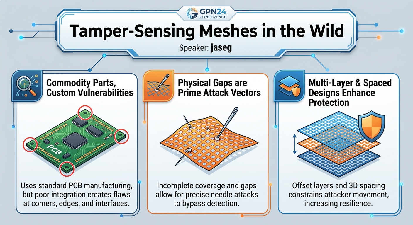
- Implement Multi-Layered and Spaced Designs: For enhanced protection, overlap multiple layers of the mesh with a 50% offset. This creates a denser, more robust protective barrier with fewer direct gaps. Furthermore, intentionally space multiple layers of meshes apart in the Z-dimension. This 3D spacing constrains an attacker's freedom of movement, making it harder to probe or drill through without detection.
- Utilize Pressure-Sensitive Connections: Incorporate pressure-sensitive connection methods to the mesh, such as tactile domes. These connections are designed to break if the device is disassembled, immediately triggering the tamper alarm. This "disassembly protection" acts as an annoying but highly effective deterrent, complicating post-disassembly analysis or manipulation.
- Continuous Monitoring with Robust Circuits: Ensure the mesh is continuously monitored by a robust circuit, ideally backed by a battery, even when the device is powered off. While simple pseudo-random bit pattern checks are common, consider more advanced techniques like Wheatstone bridge circuits for higher precision and resistance to sophisticated bypass attempts. An attacker must not only understand the mesh layout but also bypass it without triggering the alarm, often involving complex electrical manipulation under constant surveillance.
By implementing these defensive strategies, derived directly from real-world observations, manufacturers can significantly enhance the physical security of their devices against tampering attempts.
Key Takeaways
- Commodity Parts, Custom Vulnerabilities: Many tamper-sensing meshes rely on standard, off-the-shelf PCB manufacturing, but poor design choices in how these are integrated often introduce critical vulnerabilities at corners, edges, and interfaces.
- Physical Gaps are Prime Attack Vectors: Incomplete mesh coverage, non-overlapping layers, and gaps at material interfaces (e.g., PCB to mesh) are common and exploitable weaknesses, allowing for precise attacks like needle insertions to bypass detection.
- Cover Layers Need Verification: Potting and cover lacquers are vital for obfuscation, but their effectiveness depends on thorough testing for chemical resistance and complete opacity; easily removable or transparent layers offer negligible security.
- Mix Materials for Resilience: Combining tough enclosure materials with fragile, well-adhered mesh conductors significantly complicates physical tampering, as attempts to remove the enclosure or potting will likely destroy the mesh.
- 3D Protection Requires Meticulous Design: Techniques for 3D protection, such as folding or thermoforming, often introduce enlarged trace structures or gaps in curved areas, creating unintended weak points that must be addressed through careful design and manufacturing.
- Pressure-Sensitive Connections are Effective Deterrents: Simple pressure-sensitive contacts (e.g., metal domes) that break upon device disassembly provide a surprisingly effective low-tech defense, making device analysis or modification extremely difficult without triggering an alarm.
About the Speaker(s)
jaseg is a PhD candidate specializing in hardware security. They are currently in the process of finishing their doctoral thesis, which likely delves into the intricacies of physical security mechanisms like tamper-sensing meshes. Jaseg is a familiar presence at prominent technology and security events, having delivered several talks at GPN and other Chaos events, indicating a strong background and active involvement in the hacker and security research community. Their work focuses on practical, real-world analysis of security implementations in electronic devices.
Reviews
Dr. Zero (Offensive Security Researcher) — STRONG ACCEPT
Solid empirical hardware security research that actually did the work—bought 30+ devices, tore them apart, catalogued what manufacturers actually ship versus what they claim. Not a novel attack, but a valuable survey that exposes how much tamper mesh implementation relies on commodity manufacturing and how often the details get botched.
Heather Calloway (CISO) — STRONG ACCEPT
Rare empirical work on physical security controls most CISOs assume but never verify. If you have payment terminals, ATMs, HSMs, or any tamper-evident hardware in your supply chain, this changes how you should evaluate vendor claims and procurement specs.